Semiconductor Research for Nuclear and X-Ray Detectors
Since RMD’s founding in 1974, the company has rigorously engaged in semiconductor research developing materials for applications in ionizing radiation detection. Similar to its initial work with Cadmium Telluride (CdTe) detectors, this endeavor primarily focuses on room-temperature operable semiconductor detectors. These are materials that notably possess large electronic bandgaps, which intrinsically helps to minimize electronic noise without the need for cryogenic cooling. This latter characteristic, along with the materials’ high efficiency, makes them attractive for portable and handheld applications where instrument size and weight are critical design considerations. Additionally, these materials can offer greater energy resolution, or scatter rejection, because of higher conversion gains as compared to scintillation detectors.
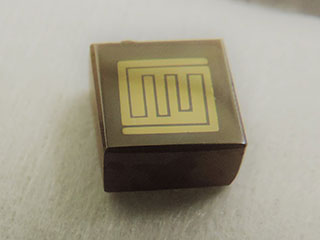
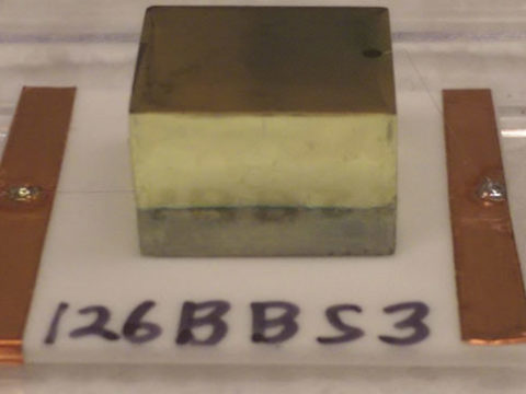
Semiconductor research involves identifying materials, developing methods to both purify and grow crystalline ingots, processing materials into operable detectors, and investigating electronics and algorithms to best extract signal data.
Material selection can originate from many sources – variants of more established (or earlier studied) compounds, theoretical modeling or literature searches. A desirable attribute is to utilize high atomic number materials that can provide efficient x- and gamma-ray detection. Analogous neutron detection schemes require materials possessing high interaction cross-sections. Electronic properties such as bandgap and charge mobility are also key factors. Motivation can also extend to pragmatic aspects of production, such as finding materials that are less costly to prepare or less susceptible to defects.
RMD generally utilizes melt-grown methods for producing ingots of semiconductors. Sizes may range from a few cm3 when first exploring electronic properties, to over a kg (in mass) for materials where large substrates are needed for imaging applications. It has also been a customary aspect of RMD’s study to employ extensive purification methods (e.g. zone refining) to improve electronic behavior.


